


LOCAL TECHNOLOGY TO TEST 12-INCH WAFERS
입력 2020.12.16 (15:12)
수정 2020.12.16 (16:45)
읽어주기 기능은 크롬기반의
브라우저에서만 사용하실 수 있습니다.
[Anchor Lead]
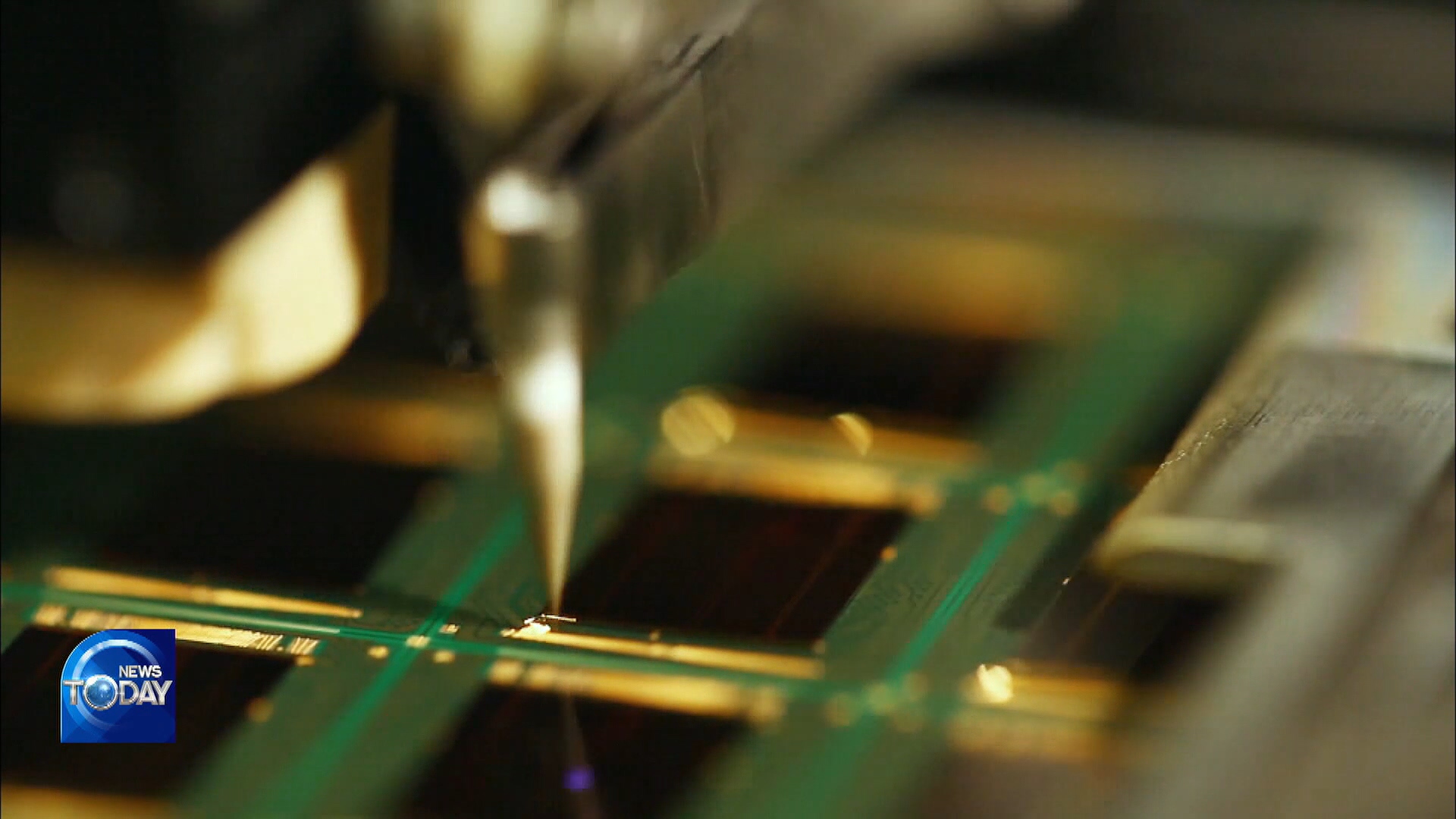
South Korea is a global leader in semiconductors but has been dependent on imports for key chip materials, components and equipment. Now, infrastructure to test the performance of 12 inch wafers has been established at home, paving the way for achieving the dream of full domestication of chip production.
[Pkg]
In July last year, Japan tightened export regulations on semiconductor parts and equipment to Korea. This dealt a severe blow to Korean chipmakers. Samsung Electronics and SK Hynix have been world-leading chip suppliers but faced with Japan’s curbs, they sorely felt the need to domestically produce related parts and materials. The argon fluoride (ArF) immersion scanner is a kep equipment in chipmaking. The scanner uses light to appraise the performance of semiconductor parts. It is the key component of what’s known as the 12-inch wafer test-bed which is a tool used to manufacture and make measurements and assessments of 12 inch wafers. The National NanoFab Center has completed the establishment of a one thousand square meter test-bed that houses ten key facilities. Some 45 billion won was invested in its construction since September last year. Korea now has the infrastructure to evaluate the performance level of semiconductor parts, materials and equipment produced by domestic firms.
[Soundbite] LEE JO-WON(PRESIDENT, NATIONAL NANOFAB CENTER) : "Dozens of tests are conducted to achieve failure-free performance. Those tests will take place here before mass production can begin."
Ever since Japan imposed export restrictions, Korea had to conduct related testing in countries such as the US and Belgium. The latest achievement removes this inconvenience.
[Soundbite] SEO DONG-CHEOL(CHIEF RESEARCHER AT CHIPMAKER) : "We can use the equipment as much as we want whenever we want. This will sharply accelerate speed in product development."
The 12 inch wafer test-bed service will start to be provided to local semiconductor parts and materials producers from as early as the start of next year.
■ 제보하기
▷ 카카오톡 : 'KBS제보' 검색, 채널 추가
▷ 전화 : 02-781-1234, 4444
▷ 이메일 : kbs1234@kbs.co.kr
▷ 유튜브, 네이버, 카카오에서도 KBS뉴스를 구독해주세요!
- LOCAL TECHNOLOGY TO TEST 12-INCH WAFERS
-
- 입력 2020-12-16 15:12:15
- 수정2020-12-16 16:45:44
[Anchor Lead]
South Korea is a global leader in semiconductors but has been dependent on imports for key chip materials, components and equipment. Now, infrastructure to test the performance of 12 inch wafers has been established at home, paving the way for achieving the dream of full domestication of chip production.
[Pkg]
In July last year, Japan tightened export regulations on semiconductor parts and equipment to Korea. This dealt a severe blow to Korean chipmakers. Samsung Electronics and SK Hynix have been world-leading chip suppliers but faced with Japan’s curbs, they sorely felt the need to domestically produce related parts and materials. The argon fluoride (ArF) immersion scanner is a kep equipment in chipmaking. The scanner uses light to appraise the performance of semiconductor parts. It is the key component of what’s known as the 12-inch wafer test-bed which is a tool used to manufacture and make measurements and assessments of 12 inch wafers. The National NanoFab Center has completed the establishment of a one thousand square meter test-bed that houses ten key facilities. Some 45 billion won was invested in its construction since September last year. Korea now has the infrastructure to evaluate the performance level of semiconductor parts, materials and equipment produced by domestic firms.
[Soundbite] LEE JO-WON(PRESIDENT, NATIONAL NANOFAB CENTER) : "Dozens of tests are conducted to achieve failure-free performance. Those tests will take place here before mass production can begin."
Ever since Japan imposed export restrictions, Korea had to conduct related testing in countries such as the US and Belgium. The latest achievement removes this inconvenience.
[Soundbite] SEO DONG-CHEOL(CHIEF RESEARCHER AT CHIPMAKER) : "We can use the equipment as much as we want whenever we want. This will sharply accelerate speed in product development."
The 12 inch wafer test-bed service will start to be provided to local semiconductor parts and materials producers from as early as the start of next year.
이 기사가 좋으셨다면
-
좋아요
0
-
응원해요
0
-
후속 원해요
0
오늘의 핫 클릭
실시간 뜨거운 관심을 받고 있는 뉴스
헤드라인
![[속보] 이 대통령 “주택 투기 수단되며 주거 불안정 <br>초래”](/data/news/2025/07/01/20250701_NWBMR4.png)
![[영상] 정성호 “검찰 해체 표현 적절치 않아…수사·기소 분리 국민 공감대”](/data/fckeditor/vod/2025/07/01/305901751367182615.png)


이 기사에 대한 의견을 남겨주세요.