


SAMSUNG ELECTRONICS’ SEMICONDUCTORS
입력 2022.07.01 (15:05)
수정 2022.07.01 (16:45)
읽어주기 기능은 크롬기반의
브라우저에서만 사용하실 수 있습니다.
[Anchor Lead]
3 nanometer is 30,000th of the thickness of human hair. Samsung Electronics has successfully begun the mass production of semiconductors containing such finite circuits. It is not only a world first but also the most advanced of all existing chip processing technologies. However there are remaining tasks to overcome such as bringing down the defect rate.
[Pkg]
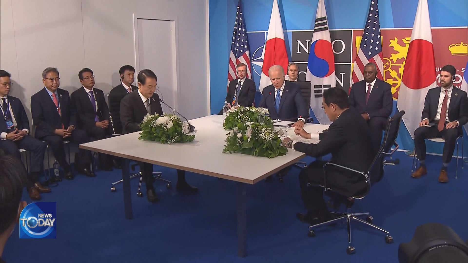
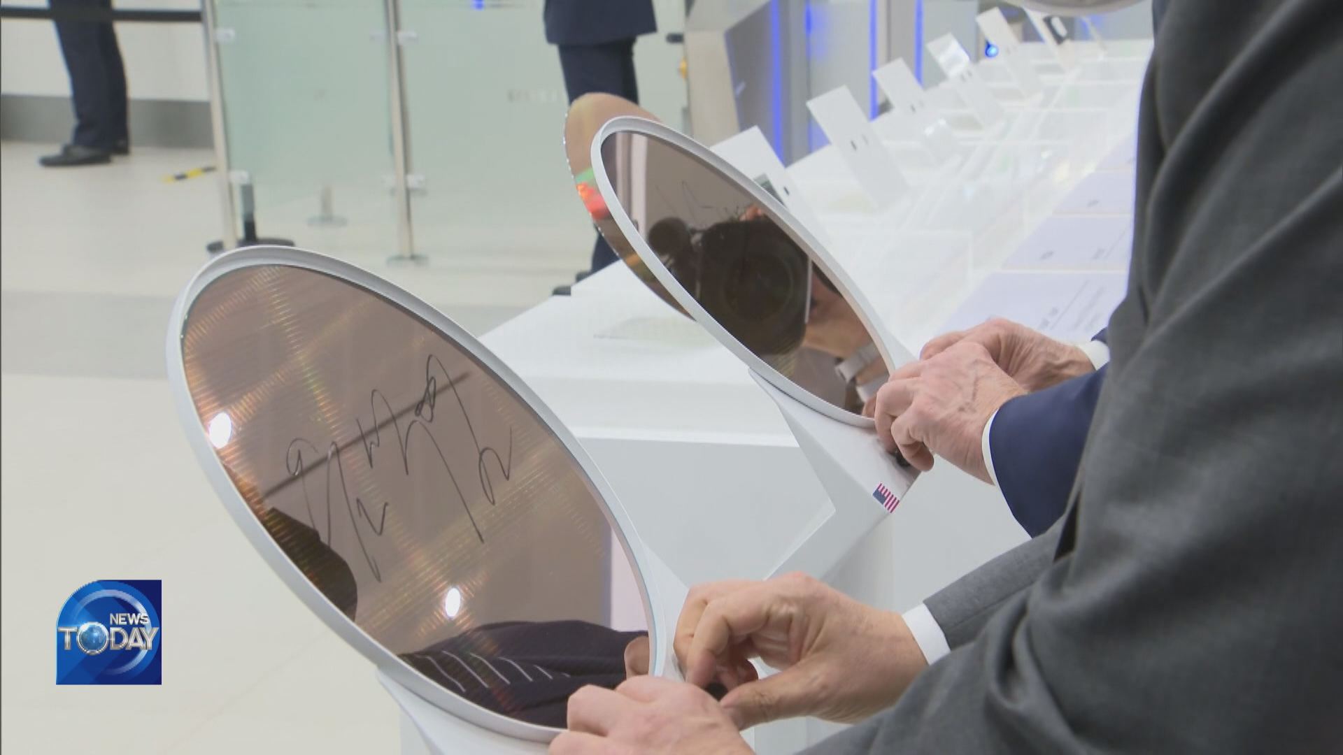
These are semiconductor wafers on which Presidents Yoon Suk-yeol and Joe Biden wrote their signatures during the U.S. leader's recent visit to South Korea. The wafers that drew global attention were none other than Samsung's 3 nanometer chips whose mass production kicked off Thursday. They were still a prototype at the time. Now, Samsung became the first in the world to begin production.
[Soundbite] Choi Si-young(President, Samsung Electronics Foundry Business) : "Samsung has posted rapid growth by preemptively introducing new tech such as EUV and is now providing the world's first 3-nano process foundry service."
3-nano chips contain electric circuits that are around one 30,000th the thickness of human hair. A new design technology of piling up electricity passageways in several layers helps ramp up data processing speed and provides greater energy efficiency. According to Samsung, compared to the 5-nanometer process, electricity use is reduced by 45% and performance is improved by 23%. One major task is bringing down the defective rate. The South Korean tech giant's 4 nanometer chips had a high defect rate.
[Soundbite] Park Gang-ho(Daishin Securities Company Researcher) : "If Samsung improves the ratio of non-defect products, it can further boost competitiveness in the foundry sector."
Another task is securing clients interested in the new product. In the global semiconductor fabrication plant or foundry market, Samsung held a market share of 16.3% in Q1, down by two percentage points on-quarter. The global leader is Taiwan's TSMC whose market share has gone up to 53.6%. Samsung Electronics is once again put to the test, as rising interest rates and recession fears around the world cast a cloud over the IT sector.
3 nanometer is 30,000th of the thickness of human hair. Samsung Electronics has successfully begun the mass production of semiconductors containing such finite circuits. It is not only a world first but also the most advanced of all existing chip processing technologies. However there are remaining tasks to overcome such as bringing down the defect rate.
[Pkg]
These are semiconductor wafers on which Presidents Yoon Suk-yeol and Joe Biden wrote their signatures during the U.S. leader's recent visit to South Korea. The wafers that drew global attention were none other than Samsung's 3 nanometer chips whose mass production kicked off Thursday. They were still a prototype at the time. Now, Samsung became the first in the world to begin production.
[Soundbite] Choi Si-young(President, Samsung Electronics Foundry Business) : "Samsung has posted rapid growth by preemptively introducing new tech such as EUV and is now providing the world's first 3-nano process foundry service."
3-nano chips contain electric circuits that are around one 30,000th the thickness of human hair. A new design technology of piling up electricity passageways in several layers helps ramp up data processing speed and provides greater energy efficiency. According to Samsung, compared to the 5-nanometer process, electricity use is reduced by 45% and performance is improved by 23%. One major task is bringing down the defective rate. The South Korean tech giant's 4 nanometer chips had a high defect rate.
[Soundbite] Park Gang-ho(Daishin Securities Company Researcher) : "If Samsung improves the ratio of non-defect products, it can further boost competitiveness in the foundry sector."
Another task is securing clients interested in the new product. In the global semiconductor fabrication plant or foundry market, Samsung held a market share of 16.3% in Q1, down by two percentage points on-quarter. The global leader is Taiwan's TSMC whose market share has gone up to 53.6%. Samsung Electronics is once again put to the test, as rising interest rates and recession fears around the world cast a cloud over the IT sector.
■ 제보하기
▷ 카카오톡 : 'KBS제보' 검색, 채널 추가
▷ 전화 : 02-781-1234, 4444
▷ 이메일 : kbs1234@kbs.co.kr
▷ 유튜브, 네이버, 카카오에서도 KBS뉴스를 구독해주세요!
- SAMSUNG ELECTRONICS’ SEMICONDUCTORS
-
- 입력 2022-07-01 15:05:35
- 수정2022-07-01 16:45:18
[Anchor Lead]
3 nanometer is 30,000th of the thickness of human hair. Samsung Electronics has successfully begun the mass production of semiconductors containing such finite circuits. It is not only a world first but also the most advanced of all existing chip processing technologies. However there are remaining tasks to overcome such as bringing down the defect rate.
[Pkg]
These are semiconductor wafers on which Presidents Yoon Suk-yeol and Joe Biden wrote their signatures during the U.S. leader's recent visit to South Korea. The wafers that drew global attention were none other than Samsung's 3 nanometer chips whose mass production kicked off Thursday. They were still a prototype at the time. Now, Samsung became the first in the world to begin production.
[Soundbite] Choi Si-young(President, Samsung Electronics Foundry Business) : "Samsung has posted rapid growth by preemptively introducing new tech such as EUV and is now providing the world's first 3-nano process foundry service."
3-nano chips contain electric circuits that are around one 30,000th the thickness of human hair. A new design technology of piling up electricity passageways in several layers helps ramp up data processing speed and provides greater energy efficiency. According to Samsung, compared to the 5-nanometer process, electricity use is reduced by 45% and performance is improved by 23%. One major task is bringing down the defective rate. The South Korean tech giant's 4 nanometer chips had a high defect rate.
[Soundbite] Park Gang-ho(Daishin Securities Company Researcher) : "If Samsung improves the ratio of non-defect products, it can further boost competitiveness in the foundry sector."
Another task is securing clients interested in the new product. In the global semiconductor fabrication plant or foundry market, Samsung held a market share of 16.3% in Q1, down by two percentage points on-quarter. The global leader is Taiwan's TSMC whose market share has gone up to 53.6%. Samsung Electronics is once again put to the test, as rising interest rates and recession fears around the world cast a cloud over the IT sector.
이 기사가 좋으셨다면
-
좋아요
0
-
응원해요
0
-
후속 원해요
0
오늘의 핫 클릭
실시간 뜨거운 관심을 받고 있는 뉴스
헤드라인


이 기사에 대한 의견을 남겨주세요.